
Introduction
While UVM is the most popular verification methodology for ASIC and FPGA development, it requires expensive SystemVerilog simulators to run. In addition, setting up a new UVM testbench is a complex task requiring specialist skill sets and the “time to first bug found” can be excessive. It is therefore no surprise that up to 70% of chip engineering budgets is spent on this task.
With Metrics DSim Cloud and Datum UVMx & Moore.io, this is no longer the case. DSIM Cloud operates in the cloud, and requires no local computing hardware. Datum UVMx & Moore.io (MIO) provide testbench code generation and a DevOps toolchain that reduces design time-to-market by up to 30% with a per-transaction Verification IP (VIP) pricing model.
This blog will give an overview of the use of these products to specify and generate a UVM test bench to verify the CORE-V MCU RTL design from the OpenHW Group.
Product Overviews
Datum Moore.io

Datum UVMx

Metrics DSim Cloud
DSim Cloud is the first and only cloud-native RTL Simulator. It combines the agility of the cloud with the high performance of a SystemVerilog and VHDL simulator, while letting you perform unlimited regression tests without licenses or upfront fees. Key simulator features include:
- SystemVerilog LRM-compliant
- VHDL 1993 and 2008
- Mixed VHDL, Verilog, and SV
- UVM, Constraint solver, SV Assertions

Reproducing the results
Getting the source code
git clone https://github.com/Datum-Technology-Corporation/core-v-mcu-uvm.git -b empty cvmcu_uvm
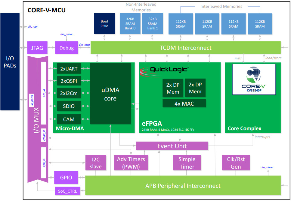
Design Under Test (DUT)
Verification Strategy

Our primary verification approach is to replace the processor core with UVM Agents that model the Instruction Fetch and Load/Store memory interfaces. As the processor core is already fully verified, this approach allows the DV team to focus their attention on the components of the CORE-V-MCU without the overhead and complexity of the core itself and its associated toolchains. APB peripherals will be explored both in sub-system and block-level environments and testbenches. Agents for driving/monitoring IO protocols JTAG, I2C, SPI, UART and SDIO as well as support (clock, reset, IRQ) and libraries (scoreboard) are Datum VIP.
This yields the following system model for the MCU, from a DV standpoint:
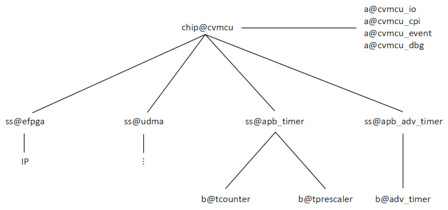
The DV specifications must therefore cover the following:
- 1 Chip: cvmcu
- 2 Sub-Systems (with internal structure)
- apb_timer
- apb_adv_timer
- 4 Agents
- cvmcu_io: transport agent to drive and monitor the MCU’s IO ports for I2C, UART, SPI, SDIO, CPI
- cvmcu_cpi: drives and monitors the Camera Parallel Interface
- cvmcu_event and cvmcu_dbg: monitor event and debug interfaces for prediction and debugging
- 3 Blocks: tcounter, tprescaler, adv_timer
DV Specifications
The Design Verification (DV) specifications are captured entirely with spreadsheets using the UVMx notation (located under /docs):
- cvmcu.uvmx.ods
- peripherals.uvmx.ods
- udma.uvmx.ods
- efpga.uvmx.ods
The specifications from the sheet “chip@cvmcu” track closely with the block diagram introduced in the previous section:
| Genre | Instance Name | IP | Configuration | Process/Part/TLM/RegMap | Description |
|---|---|---|---|---|---|
| /chip | core_v_mcu | /fsoc/core-v-mcu#sim;openhwgroup.org:systems:core-v-mcu | CORE-V-MCU | ||
| param | use_cores | bool | FALSE | Includes the Core Sub-System | |
| target | gf22fdx | use_cores | asic/gf/22fdx | Global Foundries 22nm FDX process | |
| target | nexys | use_cores | fgpa/xilinx/xc7a100t | Nexys7 | |
| target | genesys | use_cores | fgpa/xilinx/xc7k325t | Genesys | |
| ss | apb_timer | apb_timer | !is_active | Simple timer | |
| ss | apb_adv_timer | apb_adv_timer | !is_active | Advanced timer (PWM) | |
| a/mm/ctrl | jtag | datum/jtag | is_active; | #default | JTAG controller |
| a/duplex/qslv | qspi_s0 | datum/spi | is_active | (rx>a:udma_qspi0_egress); (tx>e:udma_qspi0_ingress) | QSPI slave 0 |
| a/duplex/qslv | gspi_s1 | datum/spi | is_active | (rx>a:udma_qspi1_egress); (tx>e:udma_qspi1_ingress) | QSPI slave 1 |
| a/simplex/tx | camera | cvmcu_cpi | is_active | (>e:udma_camera) | Camera Parallel Interface transmitter |
| a/duplex/slv | i2c_s0 | datum/i2c | is_active | (rx>a:udma_i2c0_egress); (tx>e:udma_i2c0_ingress) | I2C slave 0 |
| a/duplex/slv | i2c_s1 | datum/i2c | is_active | (rx>a:udma_i2c1_egress); (tx>e:udma_i2c1_ingress) | I2C slave 1 |
| a/mm | apb | datum/apb | data_width = 32; addr_width=32 | #apb_per | APB peripherals monitor |
| a/duplex | uart0 | datum/uart | is_active | (rx>a:udma_uart0_egress); (tx:e_udma_uart0_ingress) | UART 0 |
| a/duplex | uart1 | datum/uart | is_active | (rx>a:udma_uart1_egress); (tx:e_udma_uart1_ingress) | UART 1 |
| a/mm/dev | sdio | datum/sdio | is_active | #default | Flash card |
| a/duplex/mstr | i2c_m | datum/i2c | is_active | (rx>a:apb_i2c_egress); (tx>e:apb_i2c_ingress) | I2C master |
| a/duplex/board | io | cvmcu_io | is_active | (rx>a:gpio_egress); (tx>e:gpio_ingress) | IO Ports |
| a/mm/mstr | instr_obi | datum/obi | is_active=$use_cores; data_width=32; addr_width=32 | #default | Instruction memory OBI |
| a/mm/mstr | data_obi | datum/obi | is_active=$use_cores; data_width=32; addr_width=32 | #default | Data memory OBI |
| a | event | cvmcu_event | !is_active | (>mon_event); (>a:event) | Event |
| a | dbg | cvmcu_dbg | !is_active | (>mon_dbg); (>a:dbg) | Debug |
| probe | bootsel_i | in | 1 | 1 | Boot select |
| probe | stm_i | in | 1 | 0 | Structural Test Mode |
| ^ | sys_clk | sdr | 100Mhz | System | |
| ^ | jtag_clk | sdr | 50Mhz | JTAG | |
| !* | sys_reset | sync | System | ||
| ! | jtag_reset | sync | JTAG |
Code Generation
The source code (VIP) is generated by UVMx from the spreadsheet specifications:
mio gen --all *
Generated VIP:
| Agents | Environments | Testbenches |
|---|---|---|
|
|
|
Simulation and Regression
Before we can simulate, we must first install IP from the Moore.io IP server:
mio install uvmt_cvmcu_chip
To run the chip-level bit bash test in DSim interactive mode:
mio sim uvmt_cvmcu_chip -t reg_bit_bash -s 1 -a mdc
In addition to the simulation log and waveforms, UVMx provides transaction logs for ease of debugging. The following is a printout for the OBI agent log:
| TIME        | ACCESS | ADDRESS  | DATA     | BE   | ATOP | MEMTYPE | PROT |
|-------------|--------|----------|----------|------|------|---------|------|
| 20045.000ns | WRITE  | 1a105044 | 00001001 | 1111 | 00   | 0       | 0    |
| 20095.000ns | READ   | 1a105044 | 00001001 | 1111 | 00   | 0       | 0    |
| 20145.000ns | WRITE  | 1a105044 | 00001000 | 1111 | 00   | 0       | 0    |
| 20195.000ns | READ   | 1a105044 | 00001000 | 1111 | 00   | 0       | 0    |
| 20245.000ns | WRITE  | 1a105044 | 00001002 | 1111 | 00   | 0       | 0    |
| 20295.000ns | READ   | 1a105044 | 00001002 | 1111 | 00   | 0       | 0    |
| 20345.00ns  | WRITE  | 1a105044 | 00001000 | 1111 | 00   | 0       | 0    |
| 20395.000ns | READ   | 1a105044 | 00001000 | 1111 | 00   | 0       | 0    |
| 20445.000ns | WRITE  | 1a105044 | 00001004 | 1111 | 00   | 0       | 0    |
Of particular use in register tests, reg.log neatly prints out each and every access:
20045.000ns
| W | 0x1a105044 | 0x00001001 | apb_adv_timer.t1_config |
      08:00      | 0x00000001 | insel                   |
      11:08      | 0x00000000 | mode                    |
      11:11      | 0x00000000 | clksel                  |
      12:12      | 0x00000001 | updownsel               |
      24:16      | 0x00000000 | presc                   |
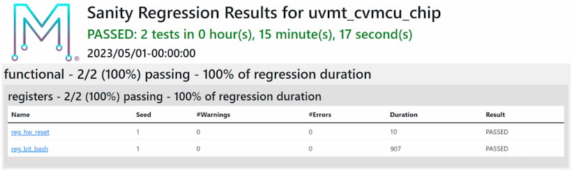
To run the chip-level sanity regression with DSim:
mio regr uvmt_cvmcu_chip sanity -a mdc
The regression report is automatically generated by the MIO CLI upon completion:
Conclusion
To learn more about the industrial-grade verification of the MCU using per-minute and per-transaction pricing models, please see the full version of this paper.